RF PCB Design Materials
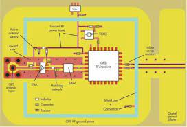
RF PCBs (radio frequency printed circuit boards) are specialized electronic components that can transmit and receive high-frequency radio signals. They are used in applications such as wireless communication systems, mobile phones, and sensors. RF PCBs operate at much higher frequencies than standard PCBs, which require careful design and construction to maintain signal integrity and minimize attenuation.
The rf pcb design process requires special attention to a variety of different parameters, including copper material selection, layer sacking, and RF circuit performance. These factors can significantly impact the quality of a final product and its ability to function properly at RF and microwave frequencies. To help ensure optimal performance, engineers use a variety of software tools to analyze different aspects of the RF PCB design. These include network analysis and time-domain reflectometry (TDR), both of which are essential for identifying impedance mismatches, signal reflections, and other factors that can cause distortion.
In addition to ensuring proper signal transmission and reducing attenuation, the RF PCB layout must also consider heat management. As RF components generate a lot of heat, it is important to use thermal vias and other methods to dissipate this energy to prevent it from damaging the PCB. In addition, RF PCBs should be placed away from heat-generating components to avoid overheating and affecting the efficiency of the system.

Types of RF PCB Design Materials
There are a few key elements to a successful RF PCB, including the substrate and copper materials used for manufacturing, as well as electrical testing and inspection techniques. During the fabrication process, RF PCBs undergo extensive automated optical inspection (AOI) and X-ray inspection to check for defects in the substrate, traces, and solder joints. These tests can detect problems such as impedance mismatches or signal reflections that can cause degraded performance or even failure. Following the PCB’s production, electrical testing such as TDR and network analysis is conducted to verify the integrity of the circuit and ensure it meets its design specifications.
Several types of RF PCBs are available for a wide range of applications. For example, flexible and wearable RF PCBs can be integrated into clothing or devices to monitor health and other data, while RF ceramic PCBs are useful for space optimization and critical RF applications.
When choosing a RF PCB substrate, it is important to select a material with a low dielectric loss tangent. High-loss materials, such as FR4, lose energy when RF signals pass through them, resulting in attenuation and distortion. Low-loss tangent materials, such as Rogers materials and Teflon, dissipate minimal energy, allowing RF signals to propagate with little degradation. These materials also have a low coefficient of thermal expansion, which is ideal for high-frequency applications.
Repairing a damaged Radio Frequency (RF) printed circuit board (PCB) is a nuanced task that involves several considerations unique to the high-frequency nature of RF circuits. While traditional PCB repairs can sometimes be straightforward, RF PCB repairs present additional challenges due to the sensitivity of RF components and the precision required in their layout.


