
flexible PCB fabrication
When it comes to fabricating flexible PCBs, there are many factors that must be taken into consideration. To make sure the board can function as intended, it must be made with quality materials and adhere to strict manufacturing standards. It is also necessary to consider how the circuit will be used and its operating environment. The circuit must be designed to withstand flexing and environmental stresses without breaking or losing its integrity.
To ensure a quality product, a flexible pcb fabrication design must go through a rigorous validation process. This includes a thorough DRC check, component and pad placement, and routing. It is also important to add labels, identifiers, and reference designators to the layout. These features will help to prevent errors during the manufacturing and assembly processes.
In addition, the design should be thoroughly inspected with simulation software or prototypes before it is ready for production. Once the design is complete, it should be generated into manufacturing files, including Gerber files. This will ensure that the design specifications are communicated accurately to manufacturers, preventing issues during production and assembly.
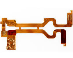
How do you validate a flexible PCB fabrication design?
The DRC check will detect any logical or electrical violations, such as incorrect connection between signal and power lines, insufficient guard traces, improper grounding connections, etc. These checks will reduce manufacturing defects and improve the overall performance of the circuit. The DRC checks will also highlight potential design flaws, such as insufficient space between traces and incorrect pad-to-via spacing. This will reduce the risk of signal interference, power noise, and other failures in the circuit.
Validating the flexible PCB fabrication design will also include an interaction with the fabricator. The fabricator will provide valuable feedback about the stiffness, bend requirements, keepout regions, material and stackup, and other critical factors to ensure the circuit can withstand bending. They can also recommend alterations to the layout to meet bending, mounting, and forming requirements.
Once the design has been validated, it is time to create the flex PCB. This will involve etching and routing the circuit, as well as forming and soldering. For flex PCBs, it is important to have positioning holes to hold the components in place during etching and assembly. These holes will be drilled in the corners of the board and are crucial to the operation of the final device.
In addition, the flex circuit must be tested for electrical continuity and power integrity. This testing is done on a jig to simulate how the final product will operate under real-world conditions. The jig is also used to test the circuit for mechanical stress. This testing is vital to the performance of a flexible circuit and should be completed before it goes into production. If any issues are discovered during this step, the flex PCB should be re-designed. A re-design will help to eliminate any errors and ensure that the flex circuit can withstand bending and forming without affecting its function. This will minimize the chances of a product failure and increase the confidence of the end user.