
Achieve High-Density Routing in PCB Fabrication Assembly
Increasingly complex electronic devices require smaller PCBs that can house more components with improved signal integrity. High-density routing, also known as HDI, is a process that achieves this by using specialized component sizes, smaller vias, and a higher connection pad density.
However, in order to ensure the successful assembly of a high-density board, there are several key factors that must be considered and implemented throughout the design and manufacturing process. This includes adherence to industry standards, meticulous attention to detail, and rigorous quality control measures.
The most important step in achieving high-density routing is properly arranging the components. This is done by first identifying the critical signal paths and then placing them in close proximity to each other. This will reduce the overall signal path length, which can minimize signal degradation, crosstalk, and interference risk.
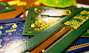
How to Achieve High-Density Routing in PCB Fabrication Assembly
Another crucial factor to consider is the choice of component types and locations. The type and quantity of components chosen will determine the overall performance of the board, which ultimately affects cost. The materials used also play an important role in this decision, as their dielectric constants will influence the speed at which signals travel through them. In addition, they will impact the design of trace widths and the locations and types of drill holes and stack-up.
Finally, the positioning of the cooling fan and ground planes will have a major effect on how the board handles heat. Strategically locating these critical elements will maximize performance and ensure that hot components do not overheat and degrade the signal. The ground planes should be large enough to act as heat sinks and distribute the heat evenly across the surface of the board.
Once the component placement is optimal, the next step in achieving high-density pcb fabrication assembly routing is to create the routing plan. This is typically done with a computer program that will calculate the maximum possible routing paths for each layer of the board. This will help the designer eliminate any potential issues with the placement of critical signals and components.
One of the most important aspects to consider in high-density PCB routing is the use of proper via design. The size and depth of the vias will have an impact on the signal propagation speed and the impedance of the signal path. For this reason, it is best to choose smaller vias that can be positioned closer to the pads to provide better performance for high-speed signal paths.
In addition to reducing the signal path length, it is also advisable to use differential pairs to improve signal quality and avoid noise coupling. Furthermore, avoiding running traces underneath sensitive components like oscillators and RF modules can prevent the potential for short circuits.
Lastly, it is vital to reserve space for test points early in the design process. This will allow for easier troubleshooting and debugging of the board during assembly. If the board is shielded, it is also a good idea to account for keepouts around these areas to avoid any unwanted connections.